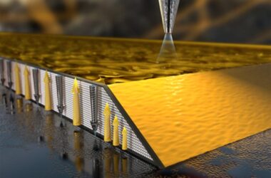

Les scientifiques du Pacific Northwest National Laboratory ont découvert de nouvelles propriétés dans un matériau semi-conducteur en utilisant une technique puissante et non conventionnelle. Crédit : Quardia, Shutterstock.com
Une découverte révèle le rôle des impuretés d’oxygène dans les propriétés des semi-conducteurs.
Une équipe de chercheurs étudiant les propriétés d’un semi-conducteur combiné à une nouvelle feuille d’oxyde mince a découvert une nouvelle source inattendue de conductivité provenant d’atomes d’oxygène piégés à l’intérieur.
Scott Chambers, spécialiste des matériaux au Pacific Northwest National Laboratory du ministère de l’énergie, a révélé les résultats de l’équipe lors de la réunion du printemps 2022 de l’American Physical Society. Les résultats de l’étude sont détaillés dans le journal .Physical Review Materials.
Cette découverte a des implications importantes pour la compréhension de la fonction des films d’oxyde minces dans la conception et la fabrication futures des semi-conducteurs. Plus précisément, les semi-conducteurs utilisés dans l’électronique moderne sont classés en deux types de base : de type n et de type p, en fonction de l’impureté électronique introduite lors de la formation du cristal. Les matériaux à base de silicium de type n et de type p sont tous deux utilisés dans les dispositifs électroniques modernes. Cependant, le développement de nouveaux types de semi-conducteurs suscite un intérêt constant. Chambers et ses collègues ont fait des expériences avec du germanium associé à une fine couche cristalline d’oxyde de lanthane-strontium-zirconium-titane (LSZTO).

Micrographie électronique à transmission à balayage de l’interface entre le germanium (en bas) et le LSZTO (en haut). Les atomes individuels sont marqués or : germanium, rouge : oxygène, vert : strontium et lanthane, bleu : titane et zirconium. Crédit : Scott Chambers, Pacific Northwest National Laboratory
“Nous avons découvert un outil puissant pour sonder la structure et la fonction des semi-conducteurs”, a déclaré Scott Chambers. “La spectroscopie photoélectronique à rayons X durs a révélé dans ce cas que les atomes d’oxygène, une impureté dans le germanium, dominent les propriétés du système matériel lorsque le germanium est joint à un matériau oxyde particulier. Ce fut une grande surprise.”
Utilisation du Diamond Light Source on the Harwell Science and Innovation Campus in Oxfordshire, England, the research team discovered they could learn a great deal more about the electronic properties of the germanium/LSZTO system than was possible using the typical methods.
“When we tried to probe the material with conventional techniques, the much higher conductivity of germanium essentially caused a short circuit,” Chambers said. “As a result, we could learn something about the electronic properties of the Ge, which we already know a lot about, but nothing about the properties of the LSZTO film or the interface between the LSZTO film and the germanium—which we suspected might be very interesting and possibly useful for technology.”

Materials Scientist Scott Chambers and his Pacific Northwest National Laboratory colleagues study the properties of semiconductor materials at atomic-level detail. Credit: Andrea Starr, Pacific Northwest National Laboratory
A new role for hard X-rays
The so-called “hard” X-rays produced by the Diamond Light Source could penetrate the material and generate information about what was going on at the atomic level.
“Our results were best interpreted in terms of oxygen impurities in the germanium being responsible for a very interesting effect,” Chambers said. “The oxygen atoms near the interface donate electrons to the LSZTO film, creating holes, or the absence of electrons, in the germanium within a few atomic layers of the interface. These specialized holes resulted in behavior that totally eclipsed the semiconducting properties of both n- and p-type germanium in the different samples we prepared. This, too, was a big surprise.”
The interface, where the thin-film oxide and the base semiconductor come together, is where interesting semiconducting properties often emerge. The challenge, according to Chambers, is to learn how to control the fascinating and potentially useful electric fields that forms at these interfaces by modifying the electric field at the surface. Ongoing experiments at PNNL are probing this possibility.
While the samples used in this research do not likely have the immediate potential for commercial use, the techniques and scientific discoveries made are expected to pay dividends in the longer term, Chambers said. The new scientific knowledge will help materials scientists and physicists better understand how to design new semiconductor material systems with useful properties.
PNNL researchers Bethany Matthews, Steven Spurgeon, Mark Bowden, Zihua Zhu and Peter Sushko contributed to the research. The study was supported by the Department of Energy Office of Science. Some experiments and sample preparation were performed at the Environmental Molecular Sciences Laboratory, a Department of Energy Office of Science user facility located at PNNL. Electron microscopy was performed in the PNNL Radiochemical Processing Laboratory. Collaborators Tien-Lin Lee and Judith Gabel performed experiments at the Diamond Light Source. Additional collaborators included the University of Texas at Arlington’s Matt Chrysler and Joe Ngai, who prepared the samples.
Reference: “Mapping hidden space-charge distributions across crystalline metal oxide/group IV semiconductor interfaces” by S. A. Chambers, M. Chrysler, J. H. Ngai, T.-L. Lee, J. Gabel, B. E. Matthews, S. R. Spurgeon, M. E. Bowden, Z. Zhu and P. V. Sushko, 21 January 2022, Physical Review Materials.
DOI: 10.1103/PhysRevMaterials.6.015002