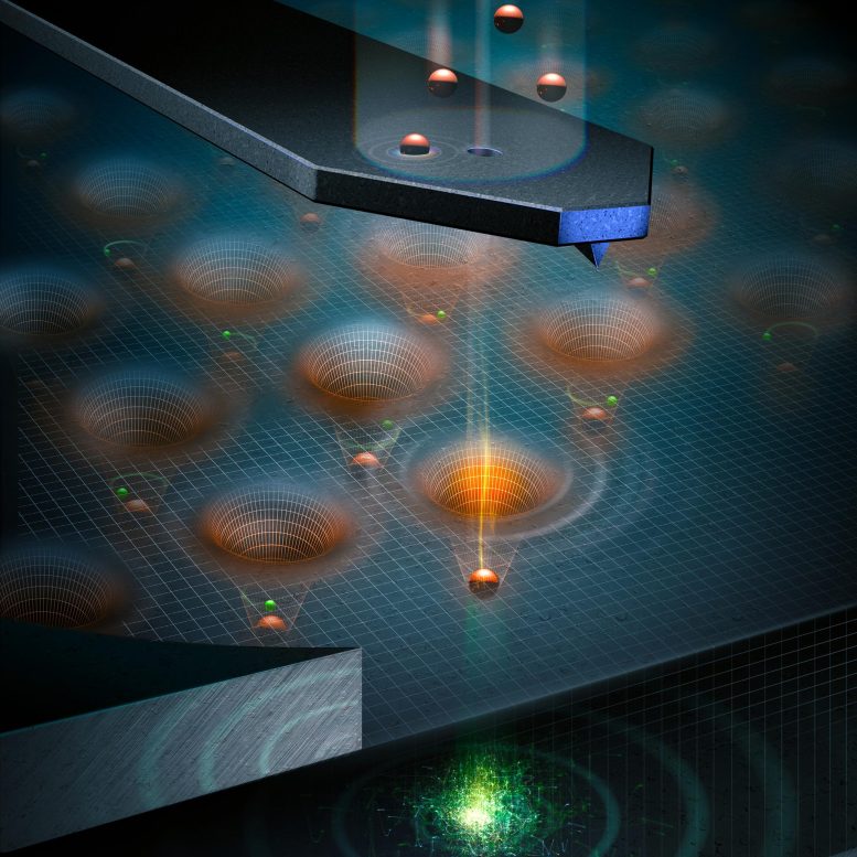
Illustration de la technique de l’atome unique. (Recadrée – cliquez sur l’image pour l’agrandir.) Crédit : David Jamieson, Université de Melbourne
Atome par atom: new silicon computer chip technique opens up quantum computing construction possibilities.
Quantum computers could be constructed cheaply and reliably using a new technique perfected by a University of Melbourne-led team that embeds single atoms in silicon wafers, one-by-one, mirroring methods used to build conventional devices, in a process outlined in an Advanced Materials paper.
The new technique – developed by Professor David Jamieson and co-authors from UNSW Sydney, Helmholtz-Zentrum Dresden-Rossendorf (HZDR), Leibniz Institute of Surface Engineering (IOM), and RMIT – can create large scale patterns of counted atoms that are controlled so their quantum states can be manipulated, coupled and read-out.
Lead author of the paper, Professor Jamieson said his team’s vision was to use this technique to build a very, very large-scale quantum device.
“We believe we ultimately could make large-scale machines based on single atom quantum bits by using our method and taking advantage of the manufacturing techniques that the semiconductor industry has perfected,” Professor Jamieson said.
La technique tire parti de la précision du microscope à force atomique, qui possède un cantilever pointu qui “touche” la surface d’une puce avec un positionnement accuracy of just half a nanometre, about the same as the spacing between atoms in a silicon crystal.
The team drilled a tiny hole in this cantilever, so that when it was showered with phosphorus atoms one would occasionally drop through the hole and embed in the silicon substrate.
The key was knowing precisely when one atom – and no more than one – had become embedded in the substrate. Then the cantilever could move to the next precise position on the array.
The team discovered that the kinetic energy of the atom as it plows into the silicon crystal and dissipates its energy by friction can be exploited to make a tiny electronic “click.”

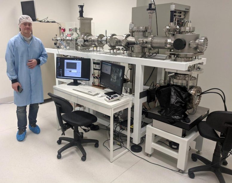
First author Dr Alexander (Melvin) Jakob stands in front of the nanostencil scanner. Credit: University of Melbourne
Professor Jamieson said the team could “hear” the electronic click as each atom dropped into one of the 10,000 sites in the prototype device.
“One atom colliding with a piece of silicon makes a very faint click, but we have invented very sensitive electronics used to detect the click, it’s much amplified and gives a loud signal, a loud and reliable signal,” Professor Jamieson said.
“That allows us to be very confident of our method. We can say, ‘Oh, there was a click. An atom just arrived. Now we can move the cantilever to the next spot and wait for the next atom,’” Professor Jamieson said.
Until now, implanting atoms in silicon has been a haphazard process, where a silicon chip gets showered with phosphorus which implants in a random pattern, like raindrops on a window.
Co-author, Scientia Professor Andrea Morello from the University of New South Wales said the new technique embedded phosphorus ions, precisely counting each one, in a silicon substrate creating a qubit “chip,” which can then be used in lab experiments to test designs for large scale devices.
“This will allow us to engineer the quantum logic operations between large arrays of individual atoms, retaining highly accurate operations across the whole processor,” Professor Morello said.
“Instead of implanting many atoms in random locations and selecting the ones that work best, they will now be placed in an orderly array, similar to the transistors in conventional semiconductors computer chips.”

Lead author Prof David Jamieson at the University of Melbourne. Credit: University of Melbourne
First author, University of Melbourne’s Dr. Alexander (Melvin) Jakob said highly specialized equipment was used for the collaboration.
“We used advanced technology developed for sensitive x-ray detectors and a special atomic force microscope originally developed for the Rosetta space mission along with a comprehensive computer model for the trajectory of ions implanted into silicon, developed in collaboration with our colleagues in Germany,” Dr. Jakob said.
“With our Centre partners, we have already produced ground-breaking results on single atom qubits made with this technique, but the new discovery will accelerate our work on large-scale devices.”
Practical implications of quantum computers include new ways of optimizing timetable and finances, unbreakable cryptography and computational drug design, and potentially the rapid development of vaccines.
Reference: “Deterministic Shallow Dopant Implantation in Silicon with Detection Confidence Upper-Bound to 99.85% by Ion–Solid Interactions” by Alexander M. Jakob, Simon G. Robson, Vivien Schmitt, Vincent Mourik, Matthias Posselt, Daniel Spemann, Brett C. Johnson, Hannes R. Firgau, Edwin Mayes, Jeffrey C. McCallum, Andrea Morello and David N. Jamieson, 11 October 2021, Advanced Materials.
DOI: 10.1002/adma.202103235
Co-authors on the report are from UNSW Sydney, Helmholtz-Zentrum Dresden-Rossendorf (HZDR), Leibniz Institute of Surface Engineering (IOM), and RMIT’s Microscopy and Microanalysis Facility.
The project was funded by the Australian Research Council Centre of Excellence for Quantum Computation and Communication Technology, the US Army Research Office, a grant from the University of Melbourne Research and Infrastructure Fund and used the facilities of the Australian National Fabrication Facility at the Melbourne Centre for Nanofabrication.


